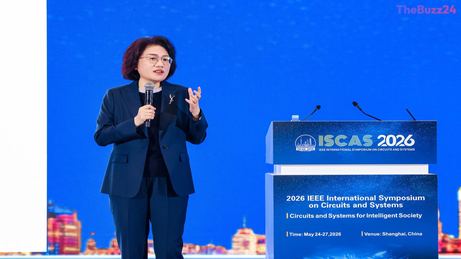
Huawei Unveils ‘LogicFolding’ Architecture to Bypass Semiconductor Manufacturing Barriers
Huawei has officially introduced a proprietary semiconductor design known as ‘LogicFolding,’ marking a strategic shift in how the company approaches hardware development. This innovative architecture utilizes a two-layer chip layout specifically engineered to optimize transistor interaction. The technology is slated for integration into the upcoming generation of Kirin smartphone processors, reflecting a broader effort to boost performance and power efficiency through structural design rather than traditional manufacturing methods.
This development is underpinned by a methodology the company calls the ‘τ Scaling Law.’ By focusing on systems-level optimizations—such as shortening wiring distances and refining memory semantics—Huawei aims to circumvent the industry-standard reliance on shrinking transistor nodes, a practice increasingly hindered by global supply chain constraints. The company notes that this framework has already been utilized in the creation of hundreds of chip variants over the last six years.
Despite the technical promise of LogicFolding, the architecture faces substantial real-world hurdles. Analysts have raised concerns regarding the thermal management of the two-layer design and the potential difficulties in achieving high manufacturing yields. Furthermore, because the company remains restricted from accessing advanced extreme ultraviolet (EUV) lithography equipment, the ability to scale this technology for high-performance AI datacenters remains uncertain. The upcoming launch of flagship devices featuring these chips will be a critical indicator of whether architectural ingenuity can successfully offset the physical limitations of current fabrication capabilities.
Key Takeaways
- Huawei's new 'LogicFolding' architecture uses a two-layer design to enhance chip performance and efficiency.
- The 'τ Scaling Law' prioritizes systems-level optimization to bypass the need for traditional transistor node shrinking.
- Mass production and thermal management remain significant challenges due to restricted access to advanced EUV lithography.
Editor’s Analysis & Impact
Huawei’s pivot to ‘LogicFolding’ is a strategic response to international trade restrictions that have limited its access to cutting-edge semiconductor manufacturing tools. By shifting the focus from physical node scaling to architectural innovation, the company is attempting to maintain its competitive edge in the mobile and AI sectors. This approach reflects a broader industry trend where design-level efficiency is becoming a primary lever for performance gains when manufacturing hardware is constrained. If successful, this strategy could lead to a divergence in global hardware standards, as companies look for ways to innovate outside of traditional Western-dominated supply chains. However, the long-term success of this initiative hinges on overcoming the thermal and yield challenges inherent in non-traditional chip layouts, which will be the ultimate test of the company’s engineering capabilities.
Frequently Asked Questions
Q: What is the main objective of the LogicFolding architecture?
A: The primary objective is to improve power efficiency and transistor interaction in mobile processors, allowing Huawei to remain competitive despite limited access to advanced manufacturing technologies.
Q: How does the 'τ Scaling Law' differ from traditional chip development?
A: Unlike traditional methods that focus on shrinking transistor sizes, the 'τ Scaling Law' emphasizes systems-level optimizations, such as reducing wiring lengths and improving memory semantics, to achieve performance improvements.
AI Disclosure: This article is based on verified data and official reports. Our Team and AI have cross-referenced every financial detail with primary sources to ensure total accuracy.
More from this Category