Next-Gen AI Chips: TSMC and Samsung Pledge Adoption of ASML’s Advanced $400 Million Lithography Tools
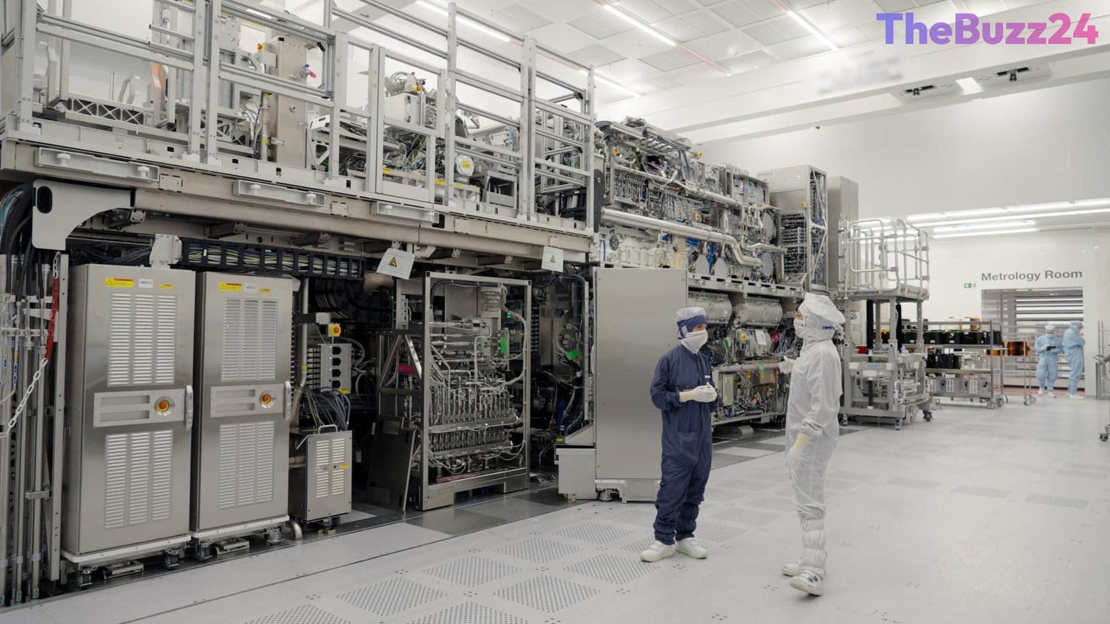
The global race for artificial intelligence supremacy is driving the world’s leading semiconductor manufacturers to secure the next generation of chipmaking technology. Industry giants Taiwan Semiconductor Manufacturing Co. (TSMC) and Samsung Electronics have officially committed to integrating ASML Holding NV’s cutting-edge High NA extreme ultraviolet (EUV) lithography machines into their future production lines. These highly sophisticated systems, which carry a price tag of approximately $400 million each, are essential for printing the ultra-fine, intricate circuit patterns required for the next wave of high-performance processors.
Samsung plans to deploy the High NA EUV technology by 2028, specifically targeting the production of advanced Dynamic Random-Access Memory (DRAM) chips. The South Korean tech giant expects this integration to significantly extend its DRAM scaling roadmap and enhance manufacturing efficiency. Meanwhile, TSMC, the world’s largest contract chipmaker, anticipates adopting the technology by 2030. TSMC’s transition is heavily driven by the increasingly complex transistor architectures necessary to power demanding AI applications, which require unprecedented levels of computational density.
By securing commitments from both TSMC and Samsung, ASML solidifies its position as the indispensable backbone of the global semiconductor supply chain. The two tech giants join Intel, which has already begun utilizing the High NA EUV systems for its own advanced manufacturing processes. To support this massive technological shift, ASML is planning to expand its total EUV manufacturing capacity by roughly 30 percent by 2027, providing much-needed visibility for long-term industry planning and capital allocation.
Beyond the machinery itself, TSMC and Samsung are also partnering with ASML on a collaborative industry initiative to transition from the current 6-inch photomask format to a next-generation 12-inch standard. Photomasks act as the master stencils used to project circuit designs onto silicon wafers. Upgrading to the larger 12-inch format is projected to dramatically boost manufacturing productivity while lowering overall chip production costs, marking a pivotal step forward for the global hardware ecosystem.
Key Takeaways
- TSMC and Samsung have committed to adopting ASML's next-generation High NA EUV lithography machines, priced at roughly $400 million per unit.
- Samsung plans to implement the technology for DRAM memory production by 2028, while TSMC targets 2030 for advanced AI-focused processors.
- The chipmakers are also collaborating with ASML to transition to larger 12-inch photomasks, aiming to lower production costs and boost efficiency.
Editor’s Analysis & Impact
The commitment of TSMC and Samsung to ASML’s High NA EUV technology marks a critical milestone for the semiconductor industry, effectively validating the massive capital expenditure required for next-generation chip fabrication. With machines costing $400 million apiece, the financial stakes are incredibly high. However, the exponential demand for AI-driven computational power has left manufacturers with little choice but to invest in tools capable of printing smaller, more complex transistor architectures. This move solidifies ASML’s monopoly on high-end lithography and provides long-term revenue visibility that will likely reassure investors. Furthermore, the transition to 12-inch photomasks highlights a broader industry push toward manufacturing efficiency to offset rising research and development costs. Ultimately, this technological leap ensures that the hardware pipeline can sustain the rapid evolution of artificial intelligence and high-performance computing over the next decade.
Frequently Asked Questions
Q: What is High NA EUV lithography, and why is it important?
A: High NA (High Numerical Aperture) EUV lithography is an advanced chipmaking technology developed by ASML. It uses extreme ultraviolet light to print incredibly small and complex circuit patterns onto silicon wafers, which is essential for manufacturing the highly dense, powerful microchips needed for AI and advanced computing.
Q: When will TSMC and Samsung begin using these new machines?
A: Samsung plans to integrate High NA EUV machines into its DRAM memory production by 2028. TSMC expects to adopt the technology for its advanced logic chips by 2030.
Q: How much do ASML's High NA EUV machines cost?
A: Each High NA EUV machine is highly complex and carries an estimated price tag of approximately $400 million.
AI Disclosure: This article is based on verified data and official reports. Our Team and AI have cross-referenced every financial detail with primary sources to ensure total accuracy.
More from this Category