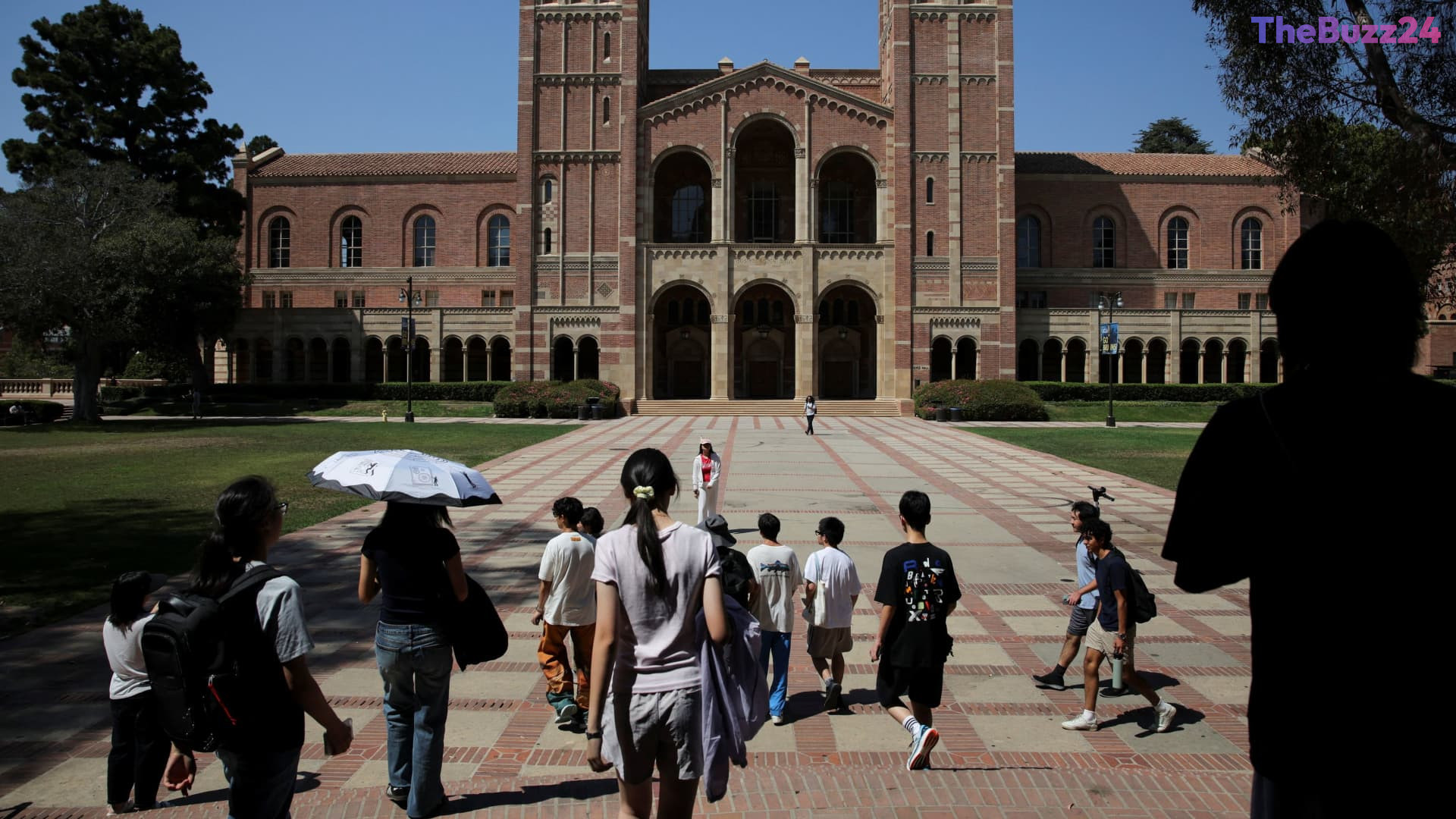
UCLA Unveils $125 Million Semiconductor Innovation Hub to Accelerate AI Hardware
The UCLA Samueli School of Engineering has launched a major $125 million semiconductor research initiative, backed by a coalition of industry titans including Meta, Broadcom, Applied Materials, GlobalFoundries, and Synopsys. This five-year collaborative project is designed to bridge the divide between theoretical academic research and practical commercial application, focusing on the entire semiconductor lifecycle from design and software development to advanced manufacturing equipment.
With the artificial intelligence sector demanding hardware that evolves faster than traditional research cycles allow, this hub aims to streamline the path from laboratory discovery to market-ready technology. By embedding industry experts directly into the academic environment, the initiative seeks to foster a more agile engineering culture capable of tackling the high-stakes technical challenges inherent in modern chip development.
Beyond its technical goals, the partnership places a heavy emphasis on cultivating the next generation of engineering talent. The funding package supports yearlong internships for doctoral students, pairing them with mentors from both the university and the participating tech firms. This dual-mentorship model is intended to equip students with the practical skills and industry insights necessary to navigate the rapidly shifting landscape of global semiconductor manufacturing.
As the industry faces mounting pressure to maintain a competitive edge in AI-powered hardware, this strategic investment serves as a vital pipeline for innovation. By integrating high-risk research into a structured academic framework, the hub aims to ensure that both the university and its corporate partners remain at the forefront of technological progress in an increasingly complex global economy.
Key Takeaways
- UCLA and a coalition of tech giants have launched a $125 million semiconductor research hub to accelerate AI hardware development.
- The initiative focuses on bridging the gap between academic research and commercial application through direct industry collaboration.
- A core component of the program is workforce development, offering doctoral students yearlong internships and dual-mentorship opportunities.
Editor’s Analysis & Impact
The establishment of this semiconductor hub represents a critical shift in how academic institutions and private industry collaborate to solve hardware bottlenecks. By pooling resources from major players like Meta and Broadcom, the initiative addresses the ‘valley of death’ often found between university research and commercialization. This model is particularly significant for the AI sector, where the pace of innovation is currently constrained by hardware limitations. From a market perspective, this partnership is a strategic move to secure domestic talent and technological superiority in a sector vital to national security and economic growth. The long-term implication is a more integrated ecosystem where research is inherently market-aware, likely leading to faster iteration cycles for next-generation chips and a more prepared workforce ready to tackle the complexities of modern semiconductor engineering.
Frequently Asked Questions
Q: Which companies are participating in the UCLA semiconductor hub?
A: The initiative is supported by a coalition including Meta, Broadcom, Applied Materials, GlobalFoundries, and Synopsys.
Q: What is the primary goal of the new research hub?
A: The hub aims to accelerate the development of next-generation semiconductor technologies, specifically for AI, by bridging the gap between academic research and commercial application.
AI Disclosure: This article is based on verified data and official reports. Our Team and AI have cross-referenced every financial detail with primary sources to ensure total accuracy.
More from this Category