NASA Warns of Hidden Dangers: Chip Resistors Prone to Cracking Under Stress
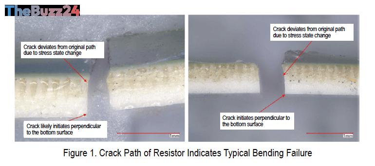
NASA’s Langley Research Center has identified a critical vulnerability in commonly used chip resistors, warning that these essential components can develop cracks under specific environmental testing conditions. While chip resistors are integral to numerous NASA projects, instances of their alumina substrates cracking during rigorous testing have been rare. However, two recent occurrences involving thick-film chip resistors revealed fractures across their short axis, a phenomenon observed after subjecting printed circuit board assemblies to vibration followed by thermal cycling.
The failures manifested as intermittent open circuit issues during high-temperature dwell periods, which would resolve as the components cooled. Detailed failure analyses have effectively ruled out manufacturing defects within the component lots or fatigue as the primary causes. Instead, the investigations pointed towards a combination of factors related to how the components are mounted and the stresses they endure on the printed circuit board.
Key contributing factors identified include the placement of relatively large resistors (case size 2512) near the board’s edge, with their longest dimension oriented parallel to the edge. This configuration, coupled with excessive solder on the component terminations and significant board flexure or twisting, creates a high-risk scenario. The way the board is rigidly mounted and the pattern of fastener torquing can further amplify these stresses, leading to bending moments that ultimately fracture the ceramic body of the resistors.
To mitigate these risks, NASA’s bulletin offers crucial guidelines for the assembly of ceramic body components onto printed circuit boards. These recommendations emphasize careful component orientation, the strategic use of finite element analysis to predict stress margins, controlled solder fillet heights to prevent direct transfer of board flexure to the ceramic, and thorough inspection of solder joints. Furthermore, functional thermal shock testing, including a hot-dwell functional test before vibration, is advised to ensure component integrity from the outset.
Key Takeaways
- Chip resistors, widely used in NASA projects, can crack due to board flexure and mounting stresses, not manufacturing defects or fatigue.
- Component placement near board edges, excessive solder, and board twisting are identified as primary risk factors.
- NASA recommends specific assembly guidelines, including component orientation, FEA, controlled solder, and functional testing, to prevent such failures.
Editor’s Analysis & Impact
This revelation from NASA highlights a critical, yet often overlooked, aspect of electronic component reliability. The findings underscore the importance of considering the entire system’s mechanical and thermal stresses, not just individual component specifications. For the aerospace and high-reliability electronics sectors, this necessitates a re-evaluation of design and assembly processes, potentially leading to increased testing costs and more sophisticated simulation techniques. The emphasis on board-level effects and mounting stresses could influence future component packaging and PCB layout best practices across the industry, aiming to enhance the resilience of sensitive electronics in demanding environments.
Frequently Asked Questions
Q: What specific type of chip resistor was found to be cracking?
A: The failures were observed in thick-film chip resistors, specifically those with a case size of 2512.
Q: What are the main causes of the chip resistor cracking?
A: The primary causes identified are bending and tensile failures resulting from printed circuit board flexure, exacerbated by component placement near board edges, excessive solder, board twisting, and mounting stresses. Manufacturing defects and fatigue were ruled out.
Q: What steps can be taken to prevent this type of cracking?
A: Recommendations include careful component orientation (avoiding long axis parallel to board edges), performing finite element analysis, controlling solder fillet height, thorough inspection of solder joints, and conducting functional thermal shock testing before vibration testing.
AI Disclosure: This article is based on verified data and official reports. Our Team and AI have cross-referenced every financial detail with primary sources to ensure total accuracy.
More from this Category